Epitaxial Thin Films and the Future of Low-Cost Solar Cells: From Lab to Market
Introduction
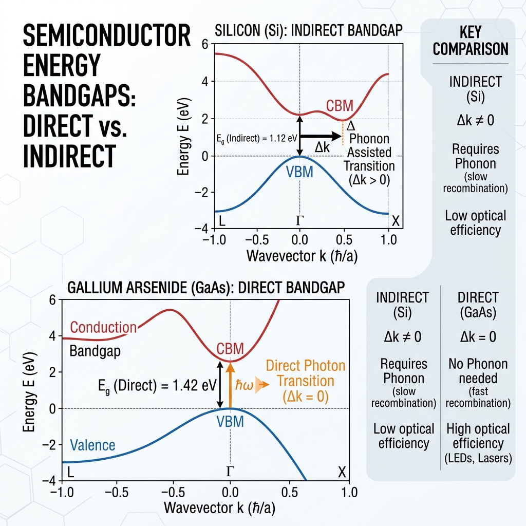
The solar energy landscape is dominated by silicon photovoltaics (PV), which account for over 95% of global installations. While silicon is abundant and mechanically robust, it is an indirect bandgap semiconductor. This fundamental physical constraint means it requires thick absorption layers (typically 150–200 micrometers) to absorb incident sunlight effectively.
To break past the theoretical limitations of silicon and lower the levelized cost of energy (LCOE), the materials science community is focusing on direct bandgap thin-film semiconductors. By utilizing epitaxial thin films, we can construct solar cells that are less than 2 micrometers thick yet convert sunlight with efficiencies exceeding 30%. In this article, we explore the synthesis, characterization, and commercialization path of epitaxial thin-film solar cells, highlighting the physics-based failure analysis required to take these materials from the lab to the factory.
Epitaxial Growth Dynamics: MBE vs. MOCVD
Epitaxy—the deposition of a crystalline overlayer on a crystalline substrate where the registry of the deposit matches that of the substrate—is key to achieving high-performance thin films. In photovoltaics, two main techniques dominate thin-film synthesis: Molecular Beam Epitaxy (MBE) and Metalorganic Chemical Vapor Deposition (MOCVD).
+--------------------------------------------------------------+
|                   Epitaxial Growth Comparison                 |
+------------------------------------+-------------------------+
| Molecular Beam Epitaxy (MBE)       | MOCVD / MOVPE           |
+------------------------------------+-------------------------+
| * Ultra-High Vacuum (~10^-11 Torr) | * Low-to-Atmospheric    |
| * Physical evaporation (Knudsen)   | * Gas-phase precursors  |
| * Atomic layer control (RHEED)     | * High throughput       |
| * Best for R&D/ideal structures   | * Industrial standard   |
+------------------------------------+-------------------------+
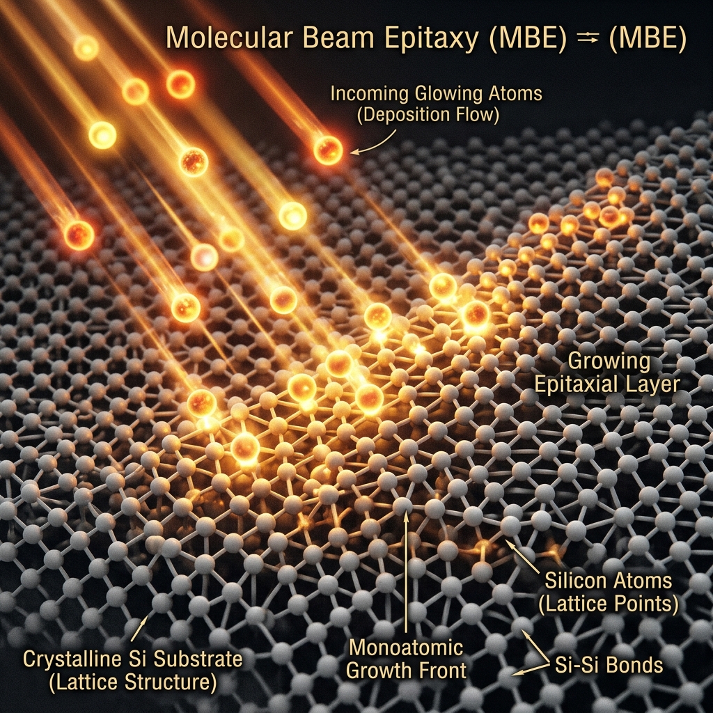
Molecular Beam Epitaxy (MBE)
MBE is a physical vapor deposition process operating under ultra-high vacuum (UHV) conditions (). Elemental sources are heated in effusion cells, generating beams of atoms or molecules that impinge on a heated substrate. The absence of gas-phase collisions allows for atomic-scale control over layer thickness and composition. Real-time monitoring is conducted via Reflection High-Energy Electron Diffraction (RHEED), letting scientists observe the layer-by-layer growth front. However, due to its high cost and low throughput, MBE is primarily restricted to academic research and specialized aerospace PV applications.
Metalorganic Chemical Vapor Deposition (MOCVD)
For commercial scaling, MOCVD (also known as MOVPE) is the industry workhorse. Instead of elemental beams, MOCVD utilizes volatile metalorganic precursors (e.g., Trimethylgallium, , and Arsine, ) carried by a gas (typically ) into a reactor chamber. The gases decompose thermally at the substrate surface, depositing epitaxial III-V compounds like Gallium Arsenide (GaAs) or Indium Gallium Phosphide (InGaP). MOCVD offers much higher deposition rates and throughput, making it the targeted technology for scaling thin-film solar cells.
Structural Defect Engineering and Characterization
A major hurdle in epitaxial thin films is lattice mismatch. If the lattice parameter of the film () differs from that of the substrate (), the growing film accumulates elastic strain energy. The lattice mismatch strain is defined as:
As the film thickness exceeds a certain "critical thickness" (), it becomes energetically favorable for the film to relieve this strain by forming misfit dislocations. These dislocations propagate through the active region of the solar cell as threading dislocations, acting as severe non-radiative recombination centers that degrade the open-circuit voltage () and short-circuit current density ().

Lattice Matched (Strained)        Exceeded Critical Thickness
  O   O   O   O   O   O            O   O   O   O   O   O
  |   |   |   |   |   |            |   |   |   |   |   |
  O---O---O---O---O---O (Film)     O---O---O   O---O---O (Misfit Dislocation)
  |   |   |   |   |   |            |   |    \ /    |   |
  X===X===X===X===X===X (Substrate) X===X====X====X===X (Substrate)
To identify and mitigate these defects, we utilize high-resolution characterization techniques:
1. High-Resolution X-Ray Diffraction (HRXRD)
By scanning the epitaxial structure with X-rays, we measure the lattice constants of the film and substrate. Bragg's Law dictates the angles at which constructive interference occurs:
From the separation of diffraction peaks (rocking curves), we calculate the residual strain, composition, and dislocation density of the grown layers. Broadening of the film's diffraction peak directly indicates structural mosaic spread and dislocation accumulation.
2. Scanning Electron Microscopy (SEM) and Cathodoluminescence
Cross-sectional SEM analysis allows us to measure film thickness, interface roughness, and layer composition using Energy-Dispersive X-ray Spectroscopy (EDS). By combining SEM with Cathodoluminescence (CL), we excite the semiconductor with an electron beam and detect the emitted light. Threading dislocations appear as dark spots or lines because they act as non-radiative recombination centers, providing a map of defect distribution across the wafer.
The Commercial Challenge: Substrate Cost Mitigation
III-V solar cells (like GaAs) hold the world record for single-junction conversion efficiency at 29.1%, compared to silicon's practical limit around 26%. However, GaAs cells cost roughly 100 times more per watt than silicon. The primary driver of this cost is not the epitaxial film itself, but the single-crystal GaAs or Ge substrate.
To bring epitaxial thin-film solar cells to market, the materials science community is actively scaling substrate reuse technologies:
- Epitaxial Lift-Off (ELO): Deposition of a thin sacrificial layer (e.g., AlAs) between the substrate and the active solar cell layers. By selectively etching the AlAs layer with hydrofluoric acid (HF), the active solar cell can be separated from the substrate and transferred to a flexible metal or plastic sheet. The parent substrate can then be repolished and reused multiple times.
- Silicon Heteroepitaxy: Direct growth of III-V materials on low-cost silicon substrates. By using graded buffer layers (e.g., GeSi), we can transition the lattice constant from silicon to III-V smoothly, confining dislocations to the inactive buffer layers.
Conclusion
Epitaxial thin films represent the frontier of solar cell technology, bridging the gap between high-cost aerospace photovoltaics and high-volume terrestrial power generation. Achieving commercial viability requires deep engineering at the intersection of crystal growth kinetics, defect thermodynamics, and microstructural failure analysis.
At Breakthrough Materials and Technology (a division of D613 Labs), we leverage our years of semiconductor laboratory expertise to help companies analyze thin-film structures, debug growth recipes, and design characterization workflows. The path from the lab to the market is paved with rigorous physics, and we are here to guide the journey.